Home
Home

The soldering kit is available HERE!
The Gerber file can be found on GitHub as a Release:
NOTE: The latest Gerber, and thus the design, includes a JLCJLCJLCJLC silkscreen label. This is used by me when ordering from JLCPCB (no endorsement nor recommendation, just what I use). If you are to use a different manufacturer, I recommend you change or remove this label in the KiCAD file or Gerber file directly.
Click on the icon bellow to be directed to this kit's source code (including the instruction's SVGs, KiCad files, etc.)
If you prefer a step-by-step instruction rather than a single drawing, then click on the link below to go to a step-by-step guide.
Currently only the main driver board has these instructions:
-> Main Board Step-By-Step Link
Below are instruction drawings
Here are the different soldering instructions (Click on one to open the image in a new tab):
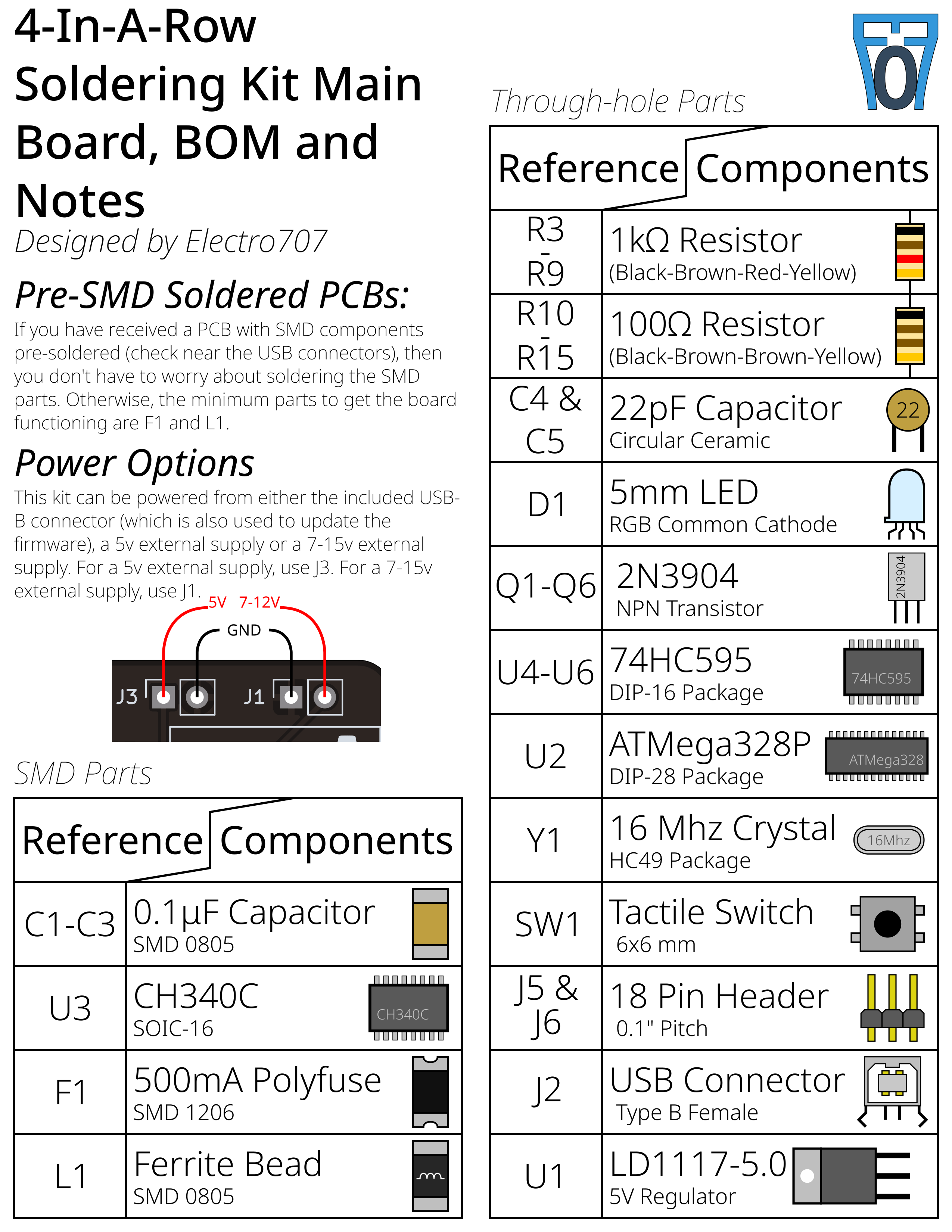
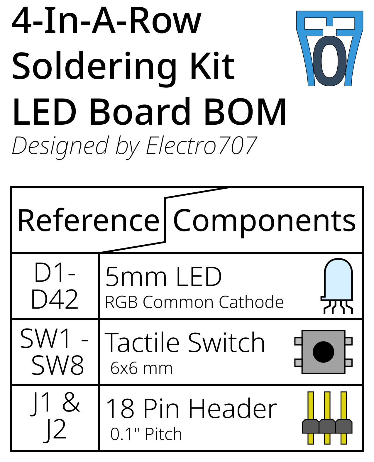
Main board Rev 1.0:
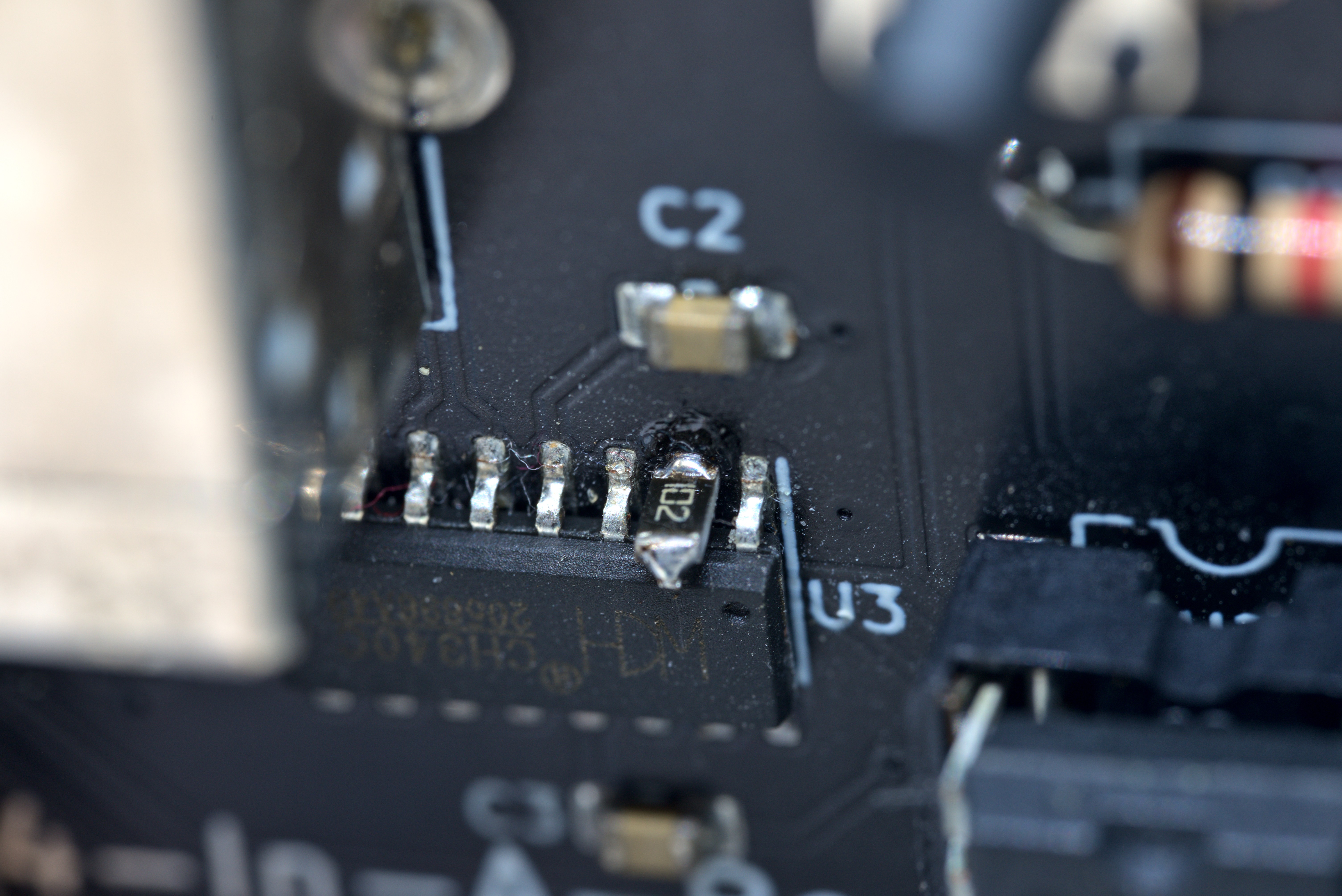
A hardware bug exists where if the CH340C is soldered, due to the CH340 pulling it's pin 2 high nominally, it conflicts when a button is pressed (which drives the pin low). This can be either mitigated by not installing the CH340, or fixed by bending CH340's pin upwards and installing a 1k resistor between the pin and the pad as shown below:
The voltage regulator, for external 7-12v operation, is an LD1117 regulator, which is not pin-compatible with the popular LM7805 regulators or similar
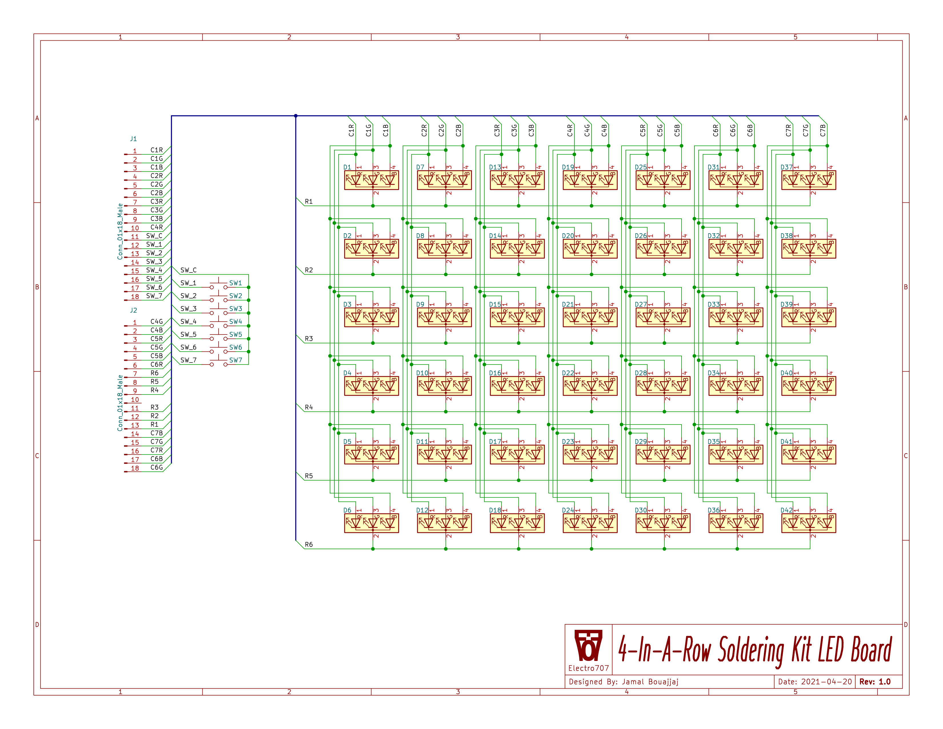
Here are the schematics for the 2 boards. Click on one for a PDF version in a new tab

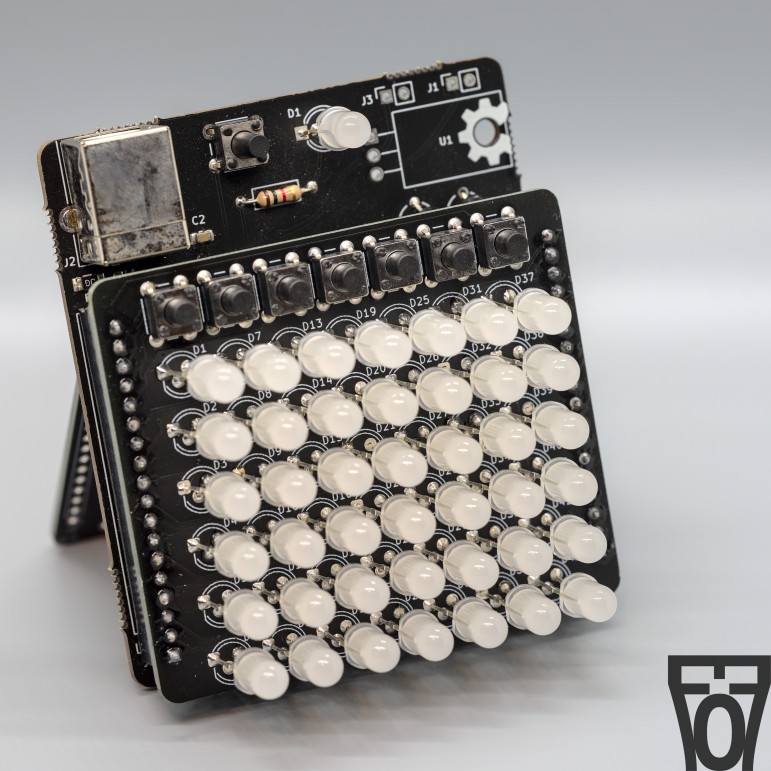
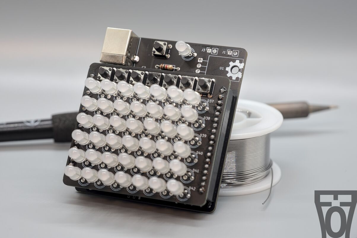
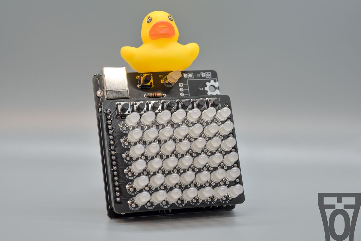
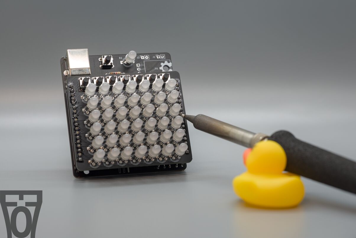
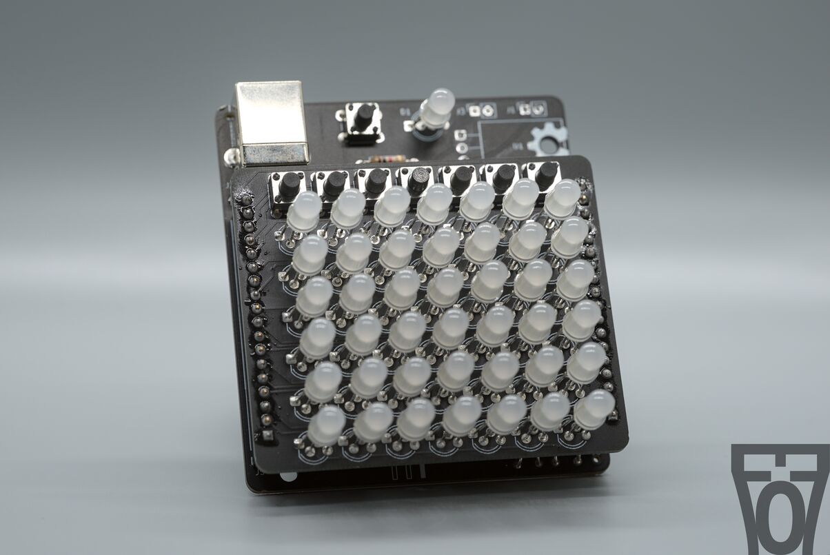
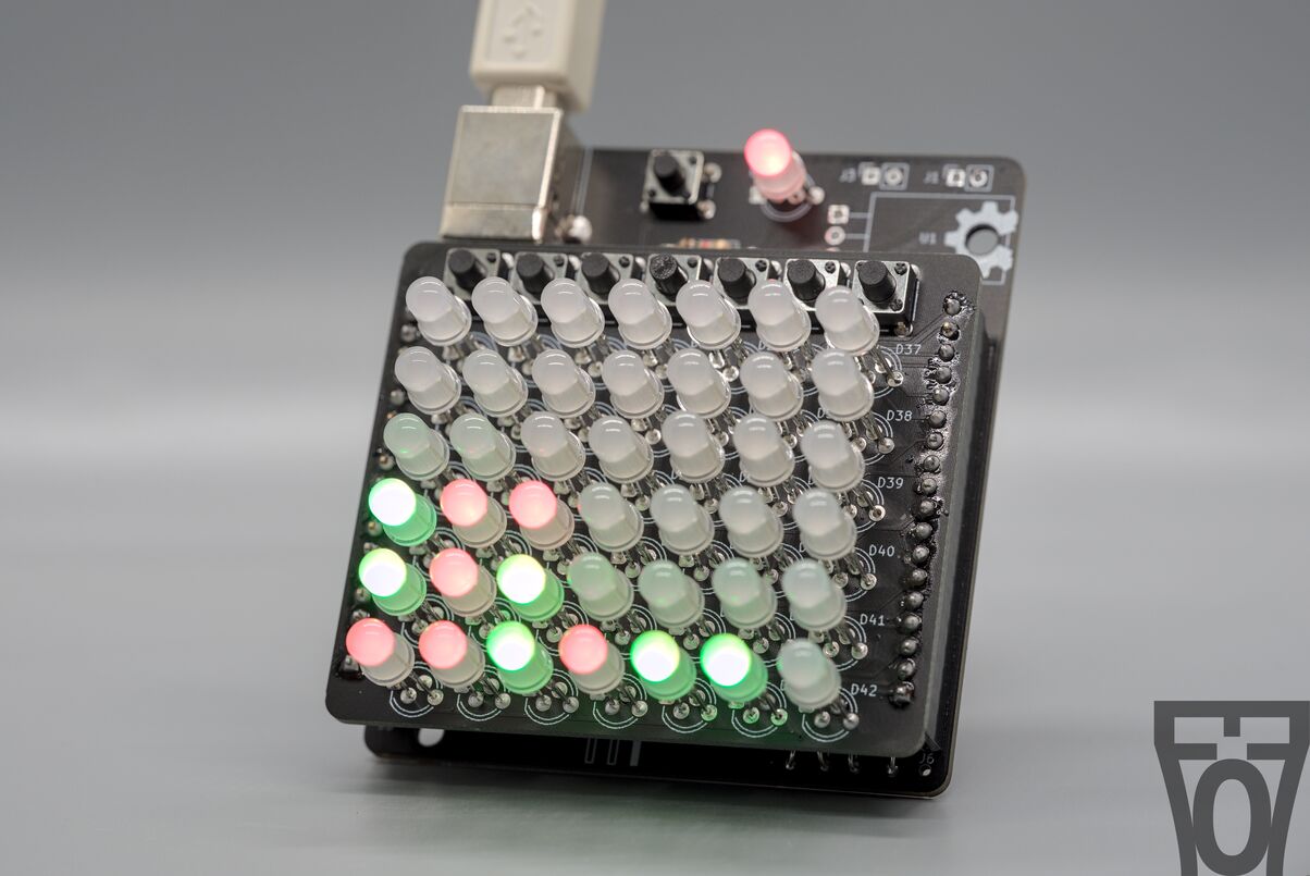
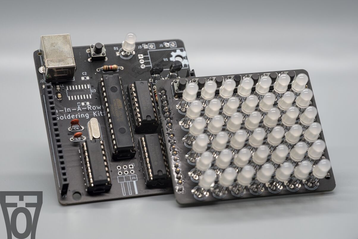
Here are some nice images I took for the kit, which could be used as a reference while troubleshooting(Click on the image to load a high-res version of it):
